
전자제품의 세계에서, PCB 트레이스는 효율적인 작동을 보장하는 데 중요한 역할을 합니다.. 인쇄 회로 기판의 이러한 경로 (PCB) 신호의 흐름을 원활하게, 힘, 및 데이터, connecting electronic components. Understanding the importance and functionality of PCB traces is crucial for engineers and designers. Proper trace width, 길이, impedance, and routing are essential. This comprehensive guide explores trace design principles, trace width calculations, suggestions for better design, and trace repair techniques.
What Is a PCB Trace?
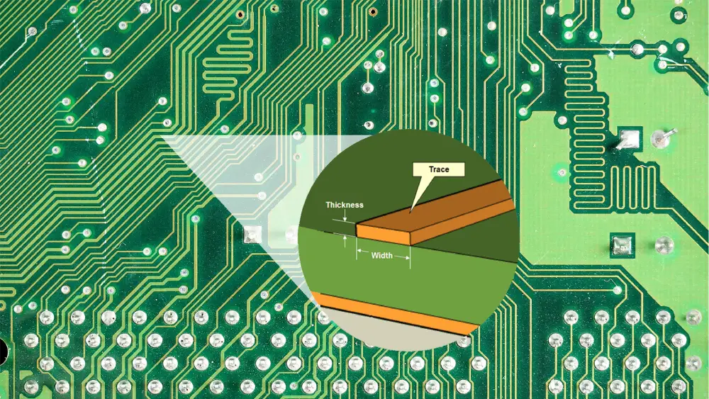
A PCB trace is a conductive pathway on a printed circuit board that connects electronic components. It is typically a thin line of copper or other conductive material that carries electrical signals between different components, such as integrated circuits, 저항기, 커패시터, 및 커넥터, PCB에. These traces are designed to transmit signals and power while maintaining specific electrical characteristics, such as impedance, signal integrity, and minimizing electromagnetic interference (EMI). The layout and design of PCB traces play a crucial role in the overall performance and functionality of electronic devices.
Understanding the PCB Trace Thickness
PCB trace thickness plays a significant role in determining the trace’s ability to carry current, handle thermal dissipation, and resist external factors. A thicker trace can carry higher current levels without overheating, reducing the risk of electrical failures. 게다가, a thicker trace can also dissipate heat more effectively, ensuring the reliability of components. 한편, a thinner trace allows for more compact designs and finer routing, but it may have limitations in terms of current-carrying capacity and heat dissipation. PCB designers and manufacturers carefully consider the specific requirements of a circuit when determining the appropriate trace thickness, balancing factors such as current requirements, space constraints, signal integrity, and thermal considerations to achieve optimal performance and reliability.
There is a range of common PCB trace thicknesses available, typically measured in inches or millimeters. 여기에는 다음이 포함됩니다. 0.008 inches to 0.240 신장 (또는 0.2 mm에 6.0 mm). Some specific examples include 0.2 mm, 0.4 mm, 0.5 mm, 0.8 mm, 1.0 mm, 1.5 mm, 2.0 mm, 2.3 mm, 등등.
How to Calculate the Trace Width of PCB
보통, we use a professional calculator to calculate the trace width based on industry standards, below we introduce the two most common standards that are IPC2221 and IPC2152:
IPC 2221:
Introduced in 1954, the IPC 2221 computer employs a combination of charts and the formula I=kΔTbAc to determine the current flowing through a trace. The value of k differs based on whether the routing is visible (0.048) or internal (0.024). The change in temperature, represented as Delta T, plays a crucial role. 추가적으로, b remains constant at 0.44, while A represents the cross-sectional area of the trace. It is important to utilize values within the specified range to achieve accurate results during the calculation process. The current should range between 0 과 35 amperes, while the copper width must not exceed 0.5 oz or fall below 3 온스. The track width selection falls within the range of 0 ...에 10.16 mm. 더욱이, the temperature fluctuates between 10 과 100 섭씨 온도.
IPC 2152:
Compared with IPC2221, the development time of IPC2152 has been updated, and the relevant parameters such as the material and thickness of the circuit board have been fully considered, so the calculation results will be more accurate. The era of depending solely on simple formulas for calculations has passed, giving way to the adoption of more sophisticated technical methods. 처음에는, a chart is utilized to establish the initial cross-sectional area. 그후, parameters are employed to derive correlation coefficients like PCB 두께. 이에 이어, the unadjusted cross-sectional area is multiplied by the coefficient, yielding the adjusted cross-sectional area.
제안 ...에 대한 더 나은 PCB Trace Design
Proper PCB trace design is critical, which affects the overall performance, 기능, and reliability of the board. Below we list some design tips:
- Routing Options
Routing can be categorized into manual wiring and automatic wiring. While automatic wiring is an integral feature of PCB design software, designers cannot solely rely on this functionality. Manual wiring is essential to unleash the designer’s creativity and flexibility, as automatic routing serves primarily as a time-saving tool.
- Choosing the Width of PCB Traces
The selection of PCB trace width holds significant importance in circuit operation. It is crucial to ensure that the width of PCB traces is appropriate to handle the capacitance and facilitate the smooth flow of current. Precise determination of the minimum width is essential to prevent circuit board overheating, which directly impacts heat management and overall performance.
- Connect to the Ground Plane
In order to ensure consistent voltage measurement across all individual PCB traces, it is important to connect each trace to the ground plane rather than a separate ground point. The ground plane serves as a common reference point for all tracks, preventing variations in voltage and resistance. 이를 달성하기 위해, it is advisable to create a solid ground plane beneath the signal-carrying path, as it can enhance resistance to noise and reduce impedance. 더욱이, placing power and ground planes in the innermost layer of the board can prevent component distortion or separation caused by board bending.
- Minimize Capacitive Coupling
To minimize the effects of capacitive coupling caused by adjacent tracks and ground planes, it is advisable to separate PCB traces dedicated to the power supply and analog signals. This segregation helps reduce unwanted capacitive coupling between the tracks above and below the ground plane. 더욱이, the use of decoupling capacitors is an effective and cost-efficient measure to mitigate capacitive coupling in practical circuit designs.
- Separate High-speed&low-speed Signals
Keep high-speed signal traces separate from low-speed signals to minimize crosstalk and interference. This can be achieved by routing traces on different layers or by using ground planes as isolation barriers.
How To Repair PCB Traces?
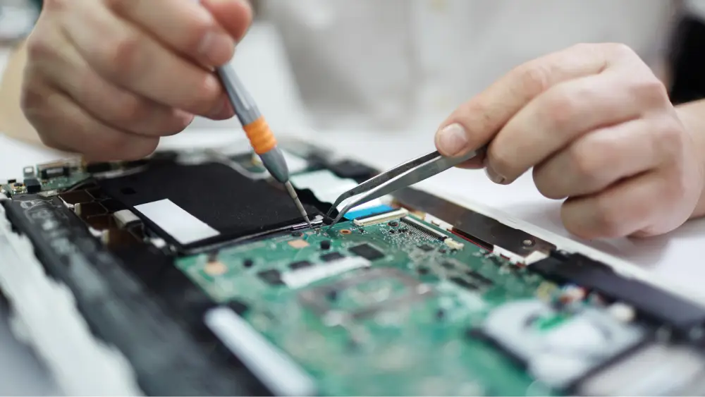
Acquiring knowledge on how to repair PCB trace issues is equally significant. When the power supply unit exhibits problems like display failure or unusual noise, it indicates the need for PCB trace repair. The following are the detailed steps for PCB trace repair:
- Begin by locating the damaged trace on the PCB.
- Carefully remove the damaged trace using a cutting tool, taking care not to harm nearby components.
- Clean the damaged areas until they display a copper color, and apply solder to the exposed regions.
- Use a cleaning paper towel or solvent cleaning pen to clean the repair area. Apply flux to the existing track and use a soldering iron to assist in soldering both sections of the track.
- Choose a suitable replacement wire that is in good condition and of the appropriate size.
- Tin the ends of the replacement wire.
- If the replacement wire is suitable, remove the insulation from both ends and solder it in place.
- Solder one end of the replacement wire. Ensure that a section of the new wire overlaps the existing trace by at least twice the width of the PCB trace. Secure the wire with tape, apply flux to the overlap, solder the wire, and trace it together.
- Shape the wire flexibly according to specific needs and requirements.
- Attach the wire securely to the surface of the circuit board using tools like tape or adhesive.
- 드디어, solder the other end of the replacement wire.
- After soldering, complete the repair process and ensure the connection is normal. Clean any remaining residue or stains.
마지막 생각들
Proper PCB trace routing ensures board performance, 신뢰할 수 있음, 비용 효율성, making PCB 설계 and manufacturing easier. 따라서, it is really necessary to understand the basic knowledge of PCB traces and routing design skills. As a leading PCB manufacturer, MOKO Technology is proficient in all aspects of circuit board knowledge, if you still have questions about PCB traces, 당신은 할 수 있습니다 우리에게 연락, and our experts will be delighted to assist you.